Best CMOS and FPGA Design flow Training in Noida & Best CMOS and FPGA Design flow Training Institute in Noida

 3.9
out of 5
based on 657 Students ratings.
3.9
out of 5
based on 657 Students ratings.
ITZIP Noida is the world-class training institute providing the best CMOS and FPGA Design flow training in Noida the present business prerequisite that empowers the candidates to achieve best employment in organizations. ITZIP Provides CMOS and FPGA Design flow training course in Noida. ITZIP is CMOS and FPGA Design flow training company Noida having more than 10 years of experience in rendering the best training service and also being the best CMOS and FPGA Design flow training institutes in Noida providing hands on training in technology by enabling the candidate to practice and work on real –time projects. ITZIP also provide its candidate with a dedicated placement team that assist and provide numerous opportunity to the candidate throughout its training period. The course structure for CMOS and FPGA Design flow training programing in Noida is intended to provide students with an efficient skills set and covers all the modules for the training program from basic to advanced level. At ITZIP CMOS and FPGA Design flow certification training in Noida is administered and overseen by technology experts from the industry having than 10+ years of experience in dealing with major CMOS and FPGA Design flow programing Live projects.
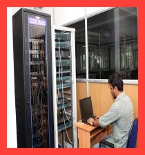
ITZIP is the best CMOS and FPGA Design flow training center in Noida with ultra-modern infrastructure and facilities established for aspirants willing to learn the skills for CMOS and FPGA Design flow that comprises of overview of CMOS and FPGA Design flow and Introduction to CMOS and FPGA Design flow, CMOS and FPGA Design flow Information radiator, CMOS and FPGA Design flow estimation, Planning, Monitoring and Adopting, CMOS and FPGA Design flow, CMOS and FPGA Design flow analysis and design, Soft skills negotiation, Value-based prioritization, CMOS and FPGA Design flow Value stream analysis, CMOS and FPGA Design flow on real time projects along with CMOS and FPGA Design flow placement training Noida. CMOS and FPGA Design flow training in Noida for beginners his being executed as per the direction of the MNC to give the best extensive knowledge of CMOS and FPGA Design flow with the industry based CMOS and FPGA Design flow course content and syllabus. The course structure is designed by the technology experts that helps in facilitating proficiency in candidates and also the training program will enable them to accomplish their objective and to get set in MNC and Big Corporations.
ITZIP is a prime CMOS and FPGA Design flow training center in Noida with advanced integrated infrastructure and new innovative labs for students to gain best insight into real working environment of IT industry. ITZIP institute in Noida prepare large number of students for the CMOS and FPGA Design flow training at a moderate value as per aspirant’s module and content requirement.
CMOS and FPGA Design flow training course in Noida involves a pragmatic approach as we believe students learn CMOS and FPGA Design flow programing the best when they practically gets involved in finding solution rather than learning theoretically ,therefore training sessions comprises of more practical sessions. This kind of practice enables candidate to gain insightful knowledge about and develop highly efficient skill set.
ITZIP is one of the best CMOS and FPGA Design flow training institute in Noida with 100% placement assistance. ITZIP has well structure modules and training program intended for both students and working professionals exclusively. At ITZIP CMOS and FPGA Design flow training is conducted during all 5 days, and special weekend CMOS and FPGA Design flow training classes in Noida can also be arranged and scheduled. We also provide CMOS and FPGA Design flow fast track training programs for students and professionals looking to upgrade themselves instantly.
Course Content and Syllabus for CMOS & FPGA Design Flow Training in Noida
CMOS & FPGA Design Flow Course Contents
- Introduction to VLSI CMOS
- MOS Fundamentals and Characterization
- NMOS/PMOS/CMOS Technologies
- Fabrication Principles
- Different Styles of Fabrication for NMOS/PMOS/CMOS
- Design with CMOS Gates
- Characterization of CMOS Circuits
- Scaling Effects
- Sub-Micron Designs
- Parasitic Extraction and Calculations
- Subsystem Design
- Layout Representation for CMOS Circuits
- Design Exercise using CMOS
- Introduction of IC Design
- Different Methodologies for IC Design
- Fabrication Flows and Fundamentals
FPGA Flow
- Re-configurable Devices, FPGA’s/CPLD’s
- Architectures of XILINX, ALTERA Devices
- Designing with FPGAs
- FPGA’s and its Design Flows
- Architecture based coding
- Efficient resource utilization
- Constrains based synthesis
- False paths and multi cycle paths
- UCF file creation
- Timing analysis/Floor Planning
- Place and route/RPM
- Back annotation, Gate level simulation, SDF Format
- DSP on FPGA
- Writing Scripts
- Hands on experience with industry Standard Tools
- ASIC Flow
Project Software Package
- Xilinx ISE
Why to Choose ITZIP for CMOS and FPGA Design flow Training in Noida
- CMOS and FPGA Design flow training in Noida is designed according to current IT market.
- Offer the best CMOS and FPGA Design flow training and placement in Noida with well defined training modules and course sessions.
- Facilitate regular, weekend and customized CMOS and FPGA Design flow training in Noida..
- One of the biggest team of Certified Expert Trainers with 5 to 15 years of Real Industry Experience.
- Mentors of CMOS and FPGA Design flow training in Noida helps in major project training, minor project training, live project preparation, interview preparation and job placement support.
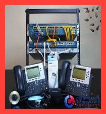
- Smart Labs with Real Latest Equipments.
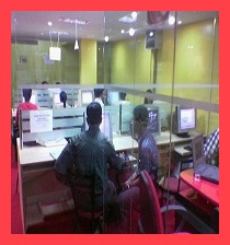
- 24x7 Lab Facilities. Students are free to access the labs for unlimited number of hours as per their own preferred timings.
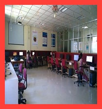
- Smart classrooms fully equipped with projectors, live racks, Wi-Fi connectivity, Digital Pads.
- Silent and Discussion Zone areas in Labs to enhance Self Study and Group Discussions.
- Free of Cost Personality Development sessions including Spoken English, Group Discussions, Mock Interviews, Presentation skills.
- Free of Cost Seminars for Personality Development & Personal Presentation.
- Varity of Study Material: Books, PDF’s, Video Lectures, Sample questions, Interview Questions (Technical and HR), and Projects.
- Hostel Facilities available at Rs 5,500/month for CMOS and FPGA Design flow Training in Noida students.
- Free Study Material, PDFs, Video Trainings, Sample Questions, Exam Preparation, Interview Questions, Lab Guides.
- Globally Recognized Course Completion Certificate.
- Extra Time Slots (E.T.S.) for Practical's(Unlimited), Absolutely Free.
- The ability to retake the class at no-charge as often as desired.
- One-on-One attention by instructors.
- Helps students to take knowledge of complex technical concepts.
- Payment options: Cheque, Cash, Credit Card, Debit card, Net Banking.
ITZIP Trainer's Profile for CMOS and FPGA Design flow Training in Noida
ITZIP'S CMOS and FPGA Design flow Trainers are:
- Are truly expert and fully up-to-date in the subjects they teach because they continue to spend time working on real-world industry applications.
- Have received awards and recognition from our partners and various recognized IT Organizations.
- Are working professionals working in multinational companies such as HCL Technologies, Birlasoft, TCS, IBM, Sapient, CMOS and FPGA Design flownt Technologies etc.
- Are certified Professionals with 7+ years of experience.
- Are Well connected with Hiring HRs in multinational companies.
Placement Assistance after CMOS and FPGA Design flow Training in Noida
ITZIP'S Placement Assistance
- ITZIP is the leader in offering placement to the students, as it has a dedicated placement wing which caters to the needs of the students during placements.
- ITZIP helps the students in the development of their RESUME as per current industry standards.
- ITZIP conducts Personality Development sessions including Spoken English, Group Discussions, Mock Interviews, Presentation skills to prepare students to face challenging interview situation with ease.
- ITZIP has prepared its students to get placed in top IT FIRMS like HCL, TCS, Infosys, Wipro, Accenture and many more.
ITZIP Course duration for CMOS and FPGA Design flow Training in Noida
- Fast Track Training Program (6+ hours daily)
- Regular Classes (Morning, Day time & Evening)
- Weekend Training Classes (Saturday, Sunday & Holidays)
Recent Placed Students


ITZIP Training Center


ITZIP Training Courses Noida
- iOS Apps Developemnt Training Noida
- Software Testing Training Noida
- QTP Training Noida
- Selenium Training Noida
- Oracle Training Noida
- STAAD.PRO Training Noida
- ANSYS Training Noida
- Appium Training Noida
- AWS Training Noida
- AUTO CAD Training Noida
- Data Warehousing Training Noida
- CAM Training Noida
- CATIA Training Noida
- Networking Training Noida
- CCNA Training Noida
- HMI Training Noida
- SAP Training Noida
- SharePoint Training Noida
- Android Training Noida
- Linux Admin Training Noida
- Cloud Computing Training Noida
- Salesforce Training Noida
- VMware Training Noida
- Embedded Systems Training Noida
- ITIL Training Noida
- PHP Training Noida
CMOS & FPGA Design Flow Training in Noida Reviews
Rating:

Rating:

Rating:
Rating:
Rating:


Enter your mobile number in 10 digits and you will be instantly connected to our customer support executive.