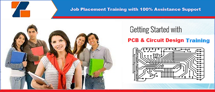
Best Projects Based Winter PCB & Circuit Design Training Institute in Noida
 4
out of 5
based on 123 ratings.
5 user reviews.
4
out of 5
based on 123 ratings.
5 user reviews.
ITZIP NOIDA offers real-time programs and job oriented training with 100 % placement assistance live project winter PCB & Circuit Design winter training in noida. Our winter certification course contains basic to advanced level knowledge, and this entire course is planned and created to get openings for work in reputed MNCs based in Noida as and when you complete the training course successfully.
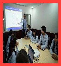
At ITZIP Noida well-equipped winter PCB & Circuit Design live project training center in Noida aspirants learn the skills for Introduction, Overview, Machines used for designing, Placing Items in the Schematic, data type, data objects, Placing Items in the Layout, Introduction to Proteus, Drilling of designed PCB. Our course on real time projects along with placement training.Our Training in Noida has been designed as per latest industry trends and keeping in mind the advanced course content and syllabus based on the professional requirement of the student; helping them to get placement in Multinational companies and achieve their career goals.
Our mentors are certified specialist and highly qualified working expert with hands on virtually multiple projects knowledge. We have structured our PCB & Circuit Design course content and syllabus as per students’ requirements to achieve their career goal.
ITZIP is one of the greatest PCB & Circuit Design training centres in Noida with world-class infrastructure and facilities and the opportunities of generating for multiple courses at Noida location. ITZIP in Noida trains thousands of individuals for PCB & Circuit Design in your budget fee parameter that is fully customized keeping in view the training and course content as per the requirements of each and every attendee.
PCB & Circuit Design involves "Learning by Doing" utilizing the most contemporary infrastructure to execute hands-on exercises and real-world simulations. This comprehensive hands-on experience in PCB & Circuit Design course ensures that each and every learner grabs the technical knowledge and skills that he or she really needs to apply while at work after getting the job in MNCs.
ITZIP's Project-based Winter Winter Training in PCB & Circuit Designing Covers the Following Modules
Winter Training in PCB & Circuit Designing is a modular winter course, regularized over 5 days a week, 2 hrs a day, and exclusively includes practical sessions. The course curriculum of Winter Training in php comprises:
PCB & Circuit Design Course Contents
- INTRODUCTION TO CIRCUIT DESIGNING
- Need of Circuit Designing
- Introduction to Basic Components like Resistor, Capacitor, Inductor etc.
- How to select components
- Basic Circuit Designing Process
INTRODUCTION TO PCB DESIGNING
- Types of PCBs
- Machines used for designing
- The Designing Process
EXPRESS SCH
- Beginning a New Schematic
- Placing Items in the Schematic
- Placing Symbols and Ports
- Labeling components
- Editing the Schematic
- Creating New Components
- Working with Sheets and Ports
- Checking the Schematic for Errors
EXPRESS PCB
- Beginning a New Layout
- Placing Items in the Layout
- Editing the Layout
- Placing Power and Ground Planes
- Changing the Board's Perimeter
- Creating New Components
- Linking the Schematic and PCB
- Keyboard Shortcuts
- Troubleshooting errors
PROTEUS
- Introduction to Proteus
- Components Libraries
- Components Properties
- Interfacing for circuitry
- Burning IC in Proteus
- Circuit Simulation
- Connection Trouble Shooting
PCB PRINTING AND ETCHING
- Introduction to printing process
- Placing of circuit on copper clad
- Etching process for final PCB
DRILLING AND SOLDERING
- Drilling of designed PCB
- Soldering Process of Components
- Testing & Troubleshooting
OTHER CAD SOFTWARES FOR PCB
- Pad2Pad
- Multisim
- Eagle
- OrCAD
Top 20 Reasons to Choose ITZIP for PCB & Circuit Design Training in Noida
- PCB & Circuit Design training in Noida is designed according to current IT market.
- Offer the best PCB & Circuit Design training and placement in Noida with well defined training modules and course sessions.
- Facilitate regular, weekend and customized PCB & Circuit Design training in Noida..
- One of the greatest team of Certified Expert Trainers with 5 to 15 years of Real Industry Experience.
- Mentors of PCB & Circuit Design training in Noida helps in major project training, minor project training, live project preparation, interview preparation and job placement support.
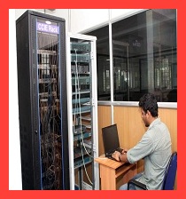
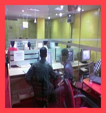
- Smart Labs with Real Latest Equipments.
- 24x7 Lab Facilities. Students are free to access the labs for unlimited number of hours as per their own preferred timings.
- Smart classrooms fully equipped with projectors, live racks, Wi-Fi connectivity, Digital Pads.
- Silent and Discussion Zone areas in Labs to enhance Self Study and Group Discussions.
- Free of Cost Personality Development sessions including Spoken English, Group Discussions, Mock Interviews, Presentation skills.
- Free of Cost Seminars for Personality Development & Personal Presentation.
- Varity of Study Material: Books, PDF’s, Video Lectures, Sample questions, Interview Questions (Technical and HR), and Projects.
- Hostel Facilities available at Rs 5,500/week for PCB & Circuit Design Training in Noida students.
- Free Study Material, PDFs, Video Trainings, Sample Questions, Exam Preparation, Interview Questions, Lab Guides.
- Globally Recognized Course Completion Certificate.
- Extra Time Slots (E.T.S.) for Practical's(Unlimited), Absolutely Free.
- The ability to retake the class at no-charge as often as desired.
- One-on-One attention by instructors.
- Helps students to take knowledge of complex technical concepts.
- Payment options: Cheque, Cash, Credit Card, Debit card, Net Banking.
6 Week Based Projects List in php Technologies
- LED Flasher
- Power Supply
- Power Supply with out transformer
- Waterlavel indicator
- Multibrator
- Rain Detector
- IR sensor Module
- Battery Tester
- Band Pass Filter
- Motor Driver Section
Placement Assistance after PCB & Circuit Design Training in Noida
ITZIP'S Placement Assistance
- ITZIP is the leader in offering placement to the students, as it has a dedicated placement wing which caters to the needs of the students during placements.
- ITZIP helps the students in the development of their RESUME as per current industry standards.
- ITZIP conducts Personality Development sessions including Spoken English, Group Discussions, Mock Interviews, Presentation skills to prepare students to face challenging interview situation with ease.
- ITZIP has prepared its students to get placed in top IT FIRMS like HCL, TCS, Infosys, Wipro, Accenture and many more.
ITZIP Course duration for PCB & Circuit Design Training in Noida
- Fast Track Training Program (6+ hours daily)
- Regular Classes (Morning, Day time & Evening)
- Weekend Training Classes (Saturday, Sunday & Holidays)
Recent Placed Students


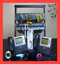
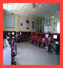
ITZIP Noida Training Center

ITZIP Training Courses Noida
- iOS Apps Developemnt Training Noida
- Software Testing Training Noida
- QTP Training Noida
- Selenium Training Noida
- Oracle Training Noida
- STAAD.PRO Training Noida
- ANSYS Training Noida
- Appium Training Noida
- AWS Training Noida
- AUTO CAD Training Noida
- Data Warehousing Training Noida
- CAM Training Noida
- CATIA Training Noida
- Networking Training Noida
- CCNA Training Noida
- HMI Training Noida
- SAP Training Noida
- SharePoint Training Noida
- Android Training Noida
- Linux Admin Training Noida
- Cloud Computing Training Noida
- Salesforce Training Noida
- VMware Training Noida
- Embedded Systems Training Noida
- ITIL Training Noida
- PHP Training Noida
PCB Circuit Design Training in Noida Reviews
Rating:

Rating:
Rating:

Rating:
Rating: